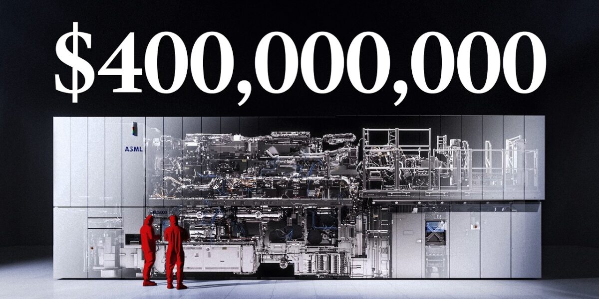
The $400 Million Machine Saving Moore’s Law
For over 50 years, Moore's Law drove technological progress. Now, a $400 million machine by ASML is the sole enabler of advanced chip manufacturing, using extreme ultraviolet lithography to overcome physical limits and continue the digital revolution.
The $400 Million Machine Saving Moore’s Law
For over half a century, the relentless march of technological progress has been dictated by Moore’s Law, an observation that the number of transistors on a microchip doubles approximately every two years. This exponential growth has fueled the digital revolution, shrinking our devices and expanding their capabilities. However, around 2015, this seemingly unstoppable trend hit a formidable barrier. The physical limits of shrinking transistors meant that traditional methods of chip manufacturing were reaching their breaking point. Yet, a single, extraordinarily complex machine, costing a staggering $400 million, has emerged as the unlikely savior of Moore’s Law, enabling the creation of the most advanced microchips humanity has ever produced.
The Heart of the Digital Age: Transistors and Lithography
At the core of every microchip lies a city of transistors, microscopic switches that control the flow of electrical signals, representing the ones and zeros that form the basis of all digital computation. The quest for more powerful chips has always been a race to make these transistors smaller. As transistors shrink, signals travel shorter distances, leading to faster processing speeds, and more transistors can be packed into the same area, exponentially increasing computing power.
The process of etching these incredibly intricate patterns onto silicon wafers is known as photolithography. This involves shining light through a mask, which contains the design of a chip layer, onto a light-sensitive material coating the wafer. The exposed areas are then removed, allowing for etching and deposition of materials to build up the chip’s structure, layer by layer. For decades, the industry relied on ultraviolet (UV) light, with the wavelength of this light directly dictating the smallest feature size that could be printed. As transistors shrunk, shorter and shorter wavelengths of UV light were employed, culminating in 193-nanometer deep UV light, which was the standard for cutting-edge chips until the mid-2010s.
The Wavelength Limit and the X-Ray Dream
The fundamental physics of light dictates that as you try to print smaller features, the wavelength of the light used becomes a critical limitation. When the wavelength of the light approaches the size of the features you’re trying to print, diffraction patterns emerge, blurring the image and preventing precise etching. To overcome this, scientists realized they needed to use much shorter wavelengths, ideally in the X-ray spectrum, around 10 nanometers, which would allow for significantly smaller transistors.
However, X-rays at these wavelengths are highly energetic and readily absorbed by air and conventional lenses. This meant that X-ray lithography would require a vacuum environment and a completely different method for focusing the light. The breakthrough came with the exploration of multi-layer mirrors, first theorized and demonstrated by scientists like Jim Underwood and Troy Barbee, and later adapted by Hiroo Kinoshita for X-ray wavelengths. These mirrors, composed of alternating layers of materials like tungsten and carbon, could reflect X-rays at specific angles. Kinoshita’s work, though met with skepticism, proved the theoretical possibility of X-ray lithography.
From Skepticism to EUV: The Birth of a New Era
The path forward was fraught with challenges. Generating the required X-ray light was difficult, often requiring massive and expensive particle accelerators. Furthermore, the mirrors needed to be extraordinarily smooth – atomically smooth – to prevent scattering of the X-ray photons. Any imperfection on the scale of the X-ray wavelength would render the mirror useless. This required manufacturing tolerances far beyond anything previously achieved.
The development eventually shifted towards Extreme Ultraviolet (EUV) lithography, utilizing wavelengths around 13.5 nanometers. This wavelength offered a compromise: short enough to print incredibly small features, yet manageable with specialized optics. Early prototypes, like the Engineering Test Stand developed by a consortium of companies, demonstrated the feasibility of EUV, but they were too slow and inefficient for mass production. The primary bottleneck was the light source and the subsequent loss of light through the numerous reflections required to direct it to the wafer.
ASML and the $400 Million Marvel
The immense complexity and cost of developing EUV technology led many companies to withdraw from the race. This left the Dutch company ASML as the sole contender. ASML, in collaboration with its German partner Zeiss, embarked on the monumental task of creating a commercial EUV lithography machine. The heart of this machine is its light source, a marvel of engineering that generates EUV light by firing a powerful laser at tiny droplets of molten tin, heating them to over 220,000 Kelvin – roughly 40 times hotter than the surface of the Sun. This process, known as laser-produced plasma, must occur 50,000 times per second, with each tin droplet precisely hit three times by lasers within microseconds.
The machine also incorporates some of the smoothest mirrors ever created. If scaled to the size of the Earth, their largest imperfection would be no thicker than a playing card. These mirrors, along with a highly precise optical system, direct the EUV light onto the chip’s mask (reticle) and then onto the wafer, all while maintaining atomic-level precision – never deviating by more than five atoms in overlaying layers. The entire system operates with components moving at accelerations exceeding 20 Gs.
The Future of Computing
This $400 million machine, the most complex commercial product ever built, is not just a piece of technology; it’s a testament to human ingenuity and perseverance. It has enabled the production of chips with features as small as 7 nanometers and is paving the way for even smaller nodes. Without ASML’s EUV lithography, Moore’s Law would have stagnated, drastically slowing down the pace of innovation in everything from artificial intelligence and smartphones to medical research and space exploration.
The continued advancement of microchip technology, driven by machines like ASML’s EUV system, promises a future of increasingly powerful, efficient, and compact devices. It underscores the critical role of fundamental scientific research and the willingness to invest in seemingly impossible engineering challenges to push the boundaries of what humanity can achieve.
Source: The World's Most Important Machine (YouTube)
Related Articles


Nvidia Earnings Signal AI Revolution’s Next Phase
Nvidia's latest earnings report reveals accelerating revenue growth and profitability, signaling a new phase in the AI revolution driven by sophisticated AI agents. The company's strong performance underscores the growing demand for computational power as AI transitions into a core digital infrastructure component.


AI’s RAM Demand Sparks Global Shortage Crisis
The insatiable demand for High Bandwidth Memory (HBM) by AI data centers has triggered a global RAM shortage, impacting everything from consumer electronics to gaming hardware. Memory manufacturers are prioritizing lucrative AI contracts, leading to price hikes and supply constraints for everyday devices.


AI Boom Sparks Unforeseen RAM Shortage and Price Hikes
The booming AI sector is driving unprecedented demand for memory, leading to a significant shortage and price hikes for RAM, particularly High Bandwidth Memory (HBM). This surge is impacting AI infrastructure costs and potentially consumer electronics.